원자력공학과, ‘원자력 안전규제라운드테이블’ 개최

연구 2026년 10월 07일 수요일

태양전지 표면에 증발시킨 물질 막 입혔더니 성능·품질 균일성 ↑

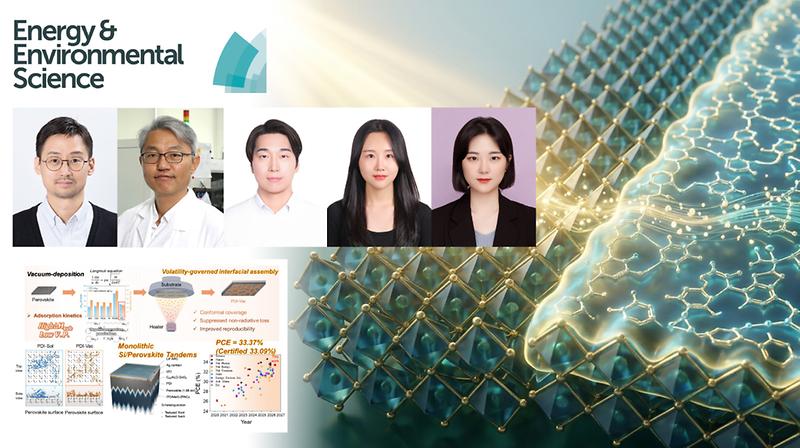
페로브스카이트 태양전지의 발전 효율과 내구성을 높이면서, 만들어지는 전지마다 성능도 균일하게 유지하는 기술이 개발됐다. 고효율 태양전지를 대량 생산하는 데 청신호가 켜졌다. UNIST 에너지화학공학과 양창덕·신소재공학과 최경진 교수팀은 특수 물질을 진공에서 휘발시켜 페로브스카이트 표면에 얇게 입힘으로써 태양전지 발전 효율과 내구성을 높였다고 20일 밝혔다. 페로브스카이트 태양전지의 페로브스카이트층과 전자수송층 사이에 패시베이션 물질이 입혀진다. 패시베이션 물질을 바르면 페로브스카이트층 상단의 결함 제거되면서 전자 손실이 줄어 태양광을 전기로 바꾸는 효율이 높아진다. 결함은 소재 손상이 시작되는 지점이기도 해서 전지 수명도 늘어난다. 이 물질은 주로 용매에 녹여 바르는데 일부가 뭉치거나 표면에 고르게 퍼지지 않아 에너지 손실이 발생하고 전지마다 성능이 들쭉날쭉해질 수 있었다. 반면 패시베이션 물질을 진공에서 가열해 휘발시킨 뒤 기체 상태의 분자가 페로브스카이트 위에 바로 내려앉도록 하면 표면에 공급되는 물질의 양과 쌓이는 속도를 조절해 균일한 막을 만들 수 있다. 이 같은 진공 증착은 균일한 막을 만들기 위해 반도체 공정 등에서도 많이 쓰이는 공정이다. 관건은 휘발 속도를 잘 제어할 수 있는 물질 자체를 찾는 일이었다. 너무 쉽게 휘발되면 표면에 쌓이는 양을 조절하기 어렵고, 반대로 잘 휘발하지 않으면 더 높은 온도로 가열해야 해 물질 자체가 분해될 수 있기 때문이다. 연구팀은 패시베이션 물질 6종의 열 안정성과 휘발 특성을 비교해 ‘피페라지늄 다이아이오다이드(PDI)’를 선정했다. 이 물질을 초당 0.01나노미터씩 쌓자 용액으로 처리했을 때보다 분자들이 표면에 더 가깝고 고르게 붙어 결함에 따른 에너지 손실을 줄였다. 이 표면 처리 기술을 적용한 페로브스카이트 태양전지의 최고 효율은 26.05%로, 같은 물질을 용액으로 처리한 전지의 25.43%보다 높았다. 페로브스카이트와 실리콘을 위아래로 쌓은 탠덤 태양전지도 33.09%의 높은 공인 효율을 기록했다. 각각 12개 전지를 제작해 비교했을 때, 전지 간 효율 편차도 줄었다. 내구성도 향상됐다. 섭씨 65도에서 빛을 계속 비추며 작동시킨 시험에서 개발한 기술을 적용한 전지는 초기 효율의 90%를 유지하는 시간이 1,005시간으로, 용액으로 처리한 전지보다 약 55% 더 길어졌다. 이번 연구는 UNIST 에너지화학공학과 박지원·김지은 연구원, 신소재공학과 노영임 연구원이 제1저자로 참여했다. 박지원 연구원은 “패시베이션 물질의 휘발성을 하나의 설계 변수로 삼아 진공에서 휘발 속도를 안정적으로 제어함으로써, 페로브스카이트 표면에 균일한 막을 만들 수 있었다”고 설명했다. 양창덕 교수는 “이번 기술은 페로브스카이트 태양전지의 효율과 내구성을 높이면서 전지 간 성능 편차도 줄일 수 있는 방법”이라며 “페로브스카이트·실리콘 탠덤 태양전지에서도 33%가 넘는 인증 효율을 확보해 고효율 태양전지의 대면적·대량 생산에 도움이 될 것으로 기대한다”고 말했다. 연구는 친환경 에너지 화학 분야 권위지 저널인 에너지와 환경 과학(Energy & Environmental Science)에 9월 1일 출판됐으며, 과학기술정보통신부 한국연구재단, 기후에너지환경부 한국에너지기술평가원의 지원을 받아 이뤄졌다.

원자력공학과, ‘원자력 안전규제라운드테이블’ 개최

연구 2026년 09월 28일 월요일

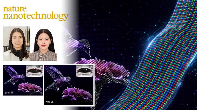
구부리고 늘려도 선명한 QLED 개발… 초고해상도 디스플레이 구현 성공

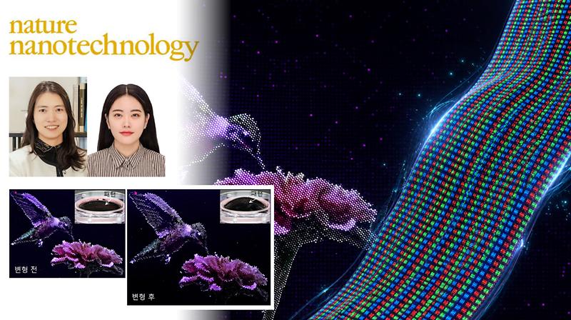
*본 보도자료는 한국연구재단 주관으로 작성되었습니다.(바로가기) □ 국내 연구진이 피부처럼 자유롭게 늘어나면서도 세계 최고 수준의 밝기와 화질을 구현하는 차세대 스트레쳐블 QLED 기술을 개발해 주목받고 있다. □ 한국연구재단(이사장 홍원화)은 UNIST 최문기 교수 연구팀이 DGIST 양지웅 교수팀, 기초과학연구원(IBS) 나노입자 연구단 김대형 부연구단장 연구팀과의 공동연구를 통해 초고해상도 스트레쳐블 QLED(양자점발광다이오드) 개발에 성공했다고 밝혔다. * 스트레쳐블 QLED : 화면을 고무줄이나 피부처럼 접거나 굴곡을 주는 것을 넘어, 상하좌우 모든 방향으로 자유롭게 늘리고 변형해도 화질 손상 없이 빛을 내는 차세대 양자점 발광 디스플레이. □ 이번 연구성과는 과학기술정보통신부와 한국연구재단이 지원하는 중견연구, 나노·소재기술개발사업 등의 지원으로 수행됐으며, 나노 분야 세계적 학술지 ‘네이처 나노테크놀로지(Nature Nanotechnology)'에 9월 14일 온라인 게재됐다. □ 기존 신축 디스플레이는 화면을 늘릴 때 발광 픽셀은 그대로 두고 배선만 늘어나는 구조적 한계가 있었다. 이로 인해 화면을 확장할수록 실제 빛이 나오는 유효 면적이 줄어들어 화질이 크게 떨어졌다. ○ 이를 해결하기 위해 픽셀 자체가 늘어나는 소재가 연구되었으나, 부드러운 특성 탓에 미세한 고해상도 패턴으로 정밀하게 가공하기 어려웠다. 또한, 전류 흐름이 원활하지 않아 야외에서 쓰기 힘들 만큼 밝기가 어둡다는 문제도 한계로 지목됐다. □ 결국 신축성을 확보하면서도 정밀한 화질과 높은 밝기를 동시에 만족시킬 혁신적인 제조 기술이 절실한 상황에서 연구팀은 초고해상도 신축 QLED 제작 공정인 ‘LIFT(Ligand engineering at the Interface and intaglio Film Transfer printing)’ 기술을 새롭게 개발했다. ○ 이 공정의 핵심은 발광층의 표면 성질을 화학적으로 정밀하게 개질하여, 계면에서의 전하 주입 효율을 대폭 향상시킴과 동시에 소재 간의 접착 특성까지 동시에 끌어올린다는 것이다. 표면 개질 기술 덕분에 전기가 매끄럽게 흐르면서도 아주 미세한 패턴까지 정밀하게 인쇄할 수 있는 공정 안정성을 확보할 수 있었다. ○ 이를 통해 약 16,000 PPI(pixel per inch)의 초고해상도 패턴 구현에 성공했다. 또한 빨강(R)·초록(G)·파랑(B) 3색 신축 발광층을 활용해 고품질 다색 화소도 구현했다. ○ 이렇게 제작된 스트레쳐블 QLED 소자는 최대 1.65배까지 늘어나도 기계적 손상이나 물리적 변형 없이 안정적으로 작동하는 뛰어난 신축성을 보여주었다. 나아가 기존 신축 발광소자들이 대부분 15,000니트 이하의 밝기에 머물렀던 것과 달리, 무려 53,300니트(nit)라는 최대 밝기를 기록하며 기존 대비 3배 이상 향상된 압도적인 성능을 증명해냈다. □ 최문기 UNIST 교수는 "이번 연구는 스트레쳐블 디스플레이의 성능을 크게 향상시키는 동시에 상용화를 위한 핵심 기술 기반을 마련한 성과로, 웨어러블 기기나 전자피부 등 차세대 소프트 전자소자 분야에 다양하게 활용될 것으로 기대한다"고 말했다.

원자력공학과, ‘원자력 안전규제라운드테이블’ 개최

연구 2026년 09월 15일 화요일

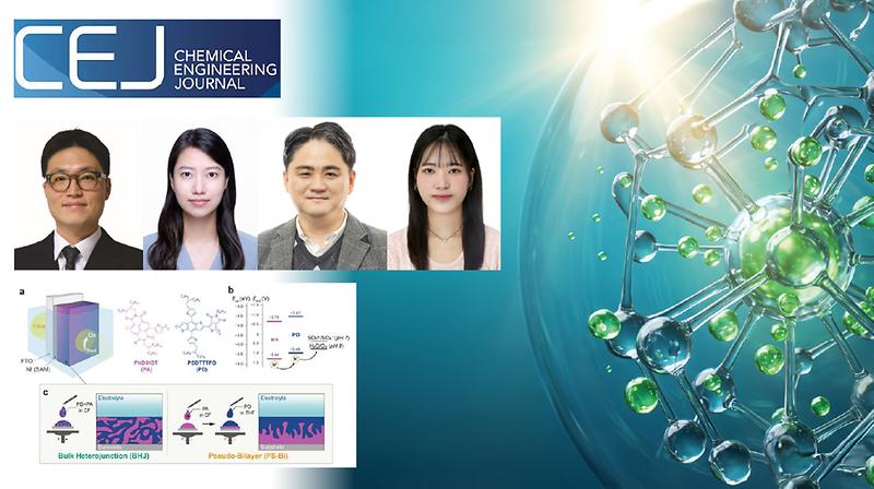
태양광 수소 생산 성능 높일 유기 반도체 광전극 개발

태양광 수전해는 햇빛으로 물을 수소와 산소로 분해해 그린 수소를 생산하는 기술이다. 물에 담긴 광전극에 햇빛을 쪼이면 햇빛을 받은 광전극이 전하 입자를 만들어내 물을 분해하는 화학반응을 일으키는 원리다. 이러한 태양광 수전해의 효율을 높이고 내구성도 뛰어난 유기반도체 광전극이 새롭게 개발됐다. UNIST 신소재공학과 조한희·최문기·송명훈 교수팀은 스위스 로잔연방공과대학교 연구진과 함께 유기반도체 공여체층과 수용체층을 차례로 쌓아 중간에 혼합층을 만드는 기술을 적용해 고성능 광양극(Photoanode)을 개발했다고 26일 밝혔다. 광전극의 일종인 광양극은 햇빛을 받아 물에서 산소를 만든다. 햇빛을 받으면 광양극 안에 양전하 입자인 정공(+)과 음전하 입자인 전자(-)가 생기는데, 정공이 물과 반응해 산소가 나온다. 나머지 전자는 광양극 아래쪽 전극과 도선을 지나 반대쪽 전극으로 전달돼 수소를 만드는 데 쓰이기 때문에 전자와 정공이 이동 과정에서 다시 합쳐지지 않도록 잘 갈라놓고, 정공은 물과 맞닿은 표면으로, 전자는 아래쪽 전극으로 보내는 것이 중요하다. 연구팀이 개발한 광양극은 유사 이중층 구조 덕분에 전자와 정공이 다시 합쳐져 사라지는 재결합 손실이 줄고, 햇빛을 받아 만들어진 더 많은 정공이 산소를 만드는 데 쓰일 수 있다. 유사 이중층 구조는 광양극의 유기반도체 수용체층과 공여체층 사이에 둘이 섞인 혼합층이 형성된 구조다. 유기 반도체 박막을 만들 때 수용체층을 먼저 쌓고 그 위에 공여체층을 올리면, 공여체층을 바르는 과정에서 공여체 용액이 아래 수용체층의 윗부분에 일부 스며들면서, 두 층 사이에 혼합물층이 생기는 ‘유사 이중층’ 구조가 만들어진다. 기존 유기반도체 광양극은 공여체와 수용체 물질을 물리적으로 섞어 하나의 혼합물층으로 만든 ‘벌크 이종접합 구조’가 사용되는데, 이는 전자와 정공을 처음 생성하는 데에는 유리했지만, 전하 이동 통로가 무분별하게 형성돼 전자와 정공이 이동하는 과정에서 다시 합쳐지기 쉬웠다. 반면 유사 이중층 구조는 중간 혼합층에서 전하가 주로 생성되고, 아래쪽 수용체층과 위쪽 공여체층이 각각 전자와 정공을 서로 다른 방향으로 보내 이러한 손실을 줄인다. 수용체와 공여체 물질을 섞는 ‘벌크 이종접합 구조’의 전하 분리 장점과, 두 물질을 위아래로 나눠 쌓는 이중층 구조의 ‘전하 이동’ 장점을 모두 갖춘 셈이다. 이 광양극은 실험에서 1.75mA/㎠의 평균 광전류 밀도를 기록했다. 이는 기존보다 약 22% 향상된 수치다. 광전류 밀도 값이 클수록 광양극에서는 산소가 더 많이 만들어진다. 산소가 생기는 물 산화 반응을 시작하기 위해 외부에서 걸어줘야 하는 전압도 0.35V에서 0.15V로 낮아져, 적은 전기에너지로 작동할 수 있었다. 또 작동 중 광전류 밀도가 0.5mA/㎠까지 떨어지는 데 걸린 시간을 기준으로 비교한 안정성도 기존보다 약 300% 향상됐다. 산화력이 강한 정공이 유기반도체를 손상시키기 쉬운데, 유사 이중층 구조 덕분에 공여체와 수용체가 맞닿는 내부 혼합층에는 손상이 덜 가기 때문이다. 조한희 교수는 “기존처럼 공여체와 수용체를 무작위로 섞은 유기 광전극은 전자와 정공이 이동하는 과정에서 손실이 크고 쉽게 성능이 떨어졌는데, 광양극 박막 안에서 두 물질의 배열을 조절함으로써 성능과 작동 안정성을 함께 높일 수 있었다”며 “낮은 전압에서도 잘 작동하는 특성이 있어 외부 전압 없이 햇빛만으로 수소를 생산하는 장치를 개발하는 데 도움이 될 것”이라고 말했다. 이번 연구 결과는 화학공학 분야의 국제 권위 학술지인 ‘케미컬 엔지니어링 저널(Chemical Engineering Journal, CEJ)’에 7월 16일 온라인 게재됐다. 연구 수행은 과학기술정보통신부 한국연구재단(NRF)의 지원사업 (No. RS-2023-00211341, RS-2025-00559676)과 이노코어(InnoCORE) 사업의 지원을 받아 진행됐다.

원자력공학과, ‘원자력 안전규제라운드테이블’ 개최

연구 2026년 09월 08일 화요일

영하 100도, 영상 100도 오가도 작동하는 페로브스카이트 태양전지 개발

영하 100도(°C)부터 영상 100도를 오가도 작동할 수 있는 고성능 페로브스카이트 태양전지가 개발됐다. 극심한 온도 변화를 견뎌야 하는 우주용 페로브스카이트 태양전지 개발에 속도가 붙을 전망이다. 페로브스카이트 태양전지는 값싸고 가벼운 차세대 전지다. 에너지화학공학과 양창덕·신승재 교수와 신소재공학과 송명훈 교수팀은 200도에 이르는 온도 변화를 반복해도 정상적으로 작동할 수 있는 고성능 페로브스카이트 태양전지를 개발했다. 위성 등이 정해진 궤도를 돌다 보면 햇빛을 직접 받는 구간과 그림자에 들어가는 구간을 반복해 지나는데, 이때 온도 차가 200도 이상 벌어진다. 우주용 태양전지 개발에서 급격한 온도 변화를 반복해서 견디는 기술이 중요한 이유다. 연구팀이 개발한 전지는 영하 100도와 영상 100도에서 각각 30분씩 두는 열순환을 16차례 반복한 뒤에도 정상적으로 작동했다. 태양전지가 태양 빛을 전기로 바꾸는 효율인 광전변환효율의 감소가 줄어, 초기 성능의 약 91%를 유지했다. 이 같은 내구성은 연구팀이 개발한 자기조립단분자막(SAM) 소재인 ‘LY-m’ 덕분이다. 자기조립단분자막은 전극과 페로브스카이트층 사이에서 전하가 이동하도록 돕는 소재로, 분자들이 전극 표면에 스스로 정렬해 분자 하나 두께의 얇은 막을 만들 수 있다. 일반적인 SAM은 온도가 크게 바뀌면 이 내부 분자들이 다시 배열되거나 서로 뭉치면서 전극을 덮는 막이 불균일해질 수 있지만, LY-m은 분자들이 전극 표면에 촘촘하고 균일하게 배열돼 열을 받아도 이러한 재배열과 응집을 억제한다. 실제로 시판 SAM 소재를 적용한 비교 전지는 같은 극한 온도 변화를 반복하자 작동하지 않았다. 제1저자인 이승록 연구원은 “‘LY-m’은 유기반도체 소재로 쓰이는 카바졸과 전극에 달라붙는 포스폰산 부분을 페녹시프로필로 연결해 만든 물질”이라며 “페녹시프로필의 벤젠 고리에서 카바졸이 붙는 위치만 조절해 분자들이 전극 위에 비스듬히 서면서 촘촘하고 균일하게 배열되도록 만들 수 있었다”고 말했다. 태양 빛을 전기로 바꾸는 효율 자체와 장기 내구성도 뛰어났다. LY-m을 적용한 태양전지는 최고 26.39%의 광전변환효율을 기록했으며 공인 인증 효율도 26.37%를 기록했다. 또한 85도에서 장시간 가열하는 시험에서는 초기 효율의 80%를 유지하는 시간이 1,994 시간에 달했다. 이번 연구는 에너지화학공학과 이승록 연구원, 신소재공학과 양진규 연구원, 에너지화학공학과 박지원 연구원이 제1저자로 참여했다. 양창덕 교수는 “분자의 구성 자체를 크게 바꾸지 않고 연결 부위의 위치만 조절해 고효율과 극한 온도 내구성을 동시에 갖춘 소재를 설계했다”며 “가볍고 공정 비용이 낮은 페로브스카이트 태양전지를 우주와 같은 극한 환경에서도 활용할 수 있도록 하는 기술의 토대가 될 것”이라고 말했다. 연구 수행은 과학기술정보통신부 한국연구재단, 이노코어InnoCORE)사업의 지원을 받아 이뤄졌으며, 국제학술지 줄(Joule)에 8월 3일 공개 됐다.

원자력공학과, ‘원자력 안전규제라운드테이블’ 개최

연구 2026년 09월 02일 수요일

“사흘 동안 소금물에 담가놔도 멀쩡”.. 고내식성 마그네슘 합금 개발

가볍지만 쉽게 삭아버려 널리 쓰이기 어려웠던 마그네슘 합금의 부식을 크게 줄이는 기술이 나왔다. 상용 합금 대비 부식 속도가 1/7 수준으로 줄었으며, 3일 동안 소금물에 담가놓아도 형태 변화 없이 멀쩡했다. UNIST 신소재공학과 박성수 교수팀은 마그네슘 속 철 불순물을 완전히 제거하는 대신 작은 입자 안에 가두는 설계 기술을 개발해 고내식성 마그네슘 합금을 만들었다고 12일 밝혔다. 마그네슘은 구조용 금속 중 가장 가볍다. 알루미늄보다 가벼워 자동차, 항공기, 드론, 휴대용 전자기기처럼 경량화가 필요한 분야에서 주목받아 왔지만, 물기나 소금기에 의해 쉽게 분해되는 탓에 널리 쓰기 어려웠다. 철 불순물은 마그네슘 합금의 부식을 빠르게 키우는 요인 중 하나다. 상용 마그네슘 원료에는 미량의 철이 들어 있는데, 철이 주변 마그네슘이 먼저 녹도록 만들어 표면을 빠르게 손상시킨다. 연구팀은 철 불순물을 입자 안에 가둠으로써 마그네슘과 직접 닿는 것을 차단하는 설계 기술을 통해 고내식성 합금을 개발했다.마그네슘 합금에 스칸듐을 미량 첨가한 기술이다. 스칸듐을 넣게 되면, 철이 스칸듐 화합물 껍질에 감싸진 ‘코어-쉘’ 구조가 만들어진다. 이 코어-쉘 구조를 만들기 위해서는 합금이 굳는 과정에서 철이 많은 코어가 먼저 생기고, 그 위를 철이 거의 없는 껍질이 덮어야 한다. 연구팀은 여러 원소를 대상으로 이론 계산을 한 뒤, 적합한 첨가물로 스칸듐을 골랐다. 실험 결과, 스칸듐을 넣지 않은 같은 마그네슘-알루미늄 합금은 3일 동안 소금물에 담그자 심하게 녹아버렸지만, 스칸듐을 넣은 합금은 큰 형태 변화가 없었다. 무게 변화로 계산한 부식 속도도 22.2mm/y에서 0.38mm/y로 낮아져, 약 60분의 1 수준에 그쳤다. mm/y는 부식 속도를 나타내는 단위로, 같은 속도로 1년 동안 부식됐을 때 금속 두께가 몇 mm 줄어드는지를 뜻한다. 또 상용 마그네슘 합금에 극미량의 스칸듐을 넣는 것만으로도 부식 속도가 1/7 수준으로 늦춰졌다. 상용 마그네슘 합금은 알루미늄 외에도 망간, 아연 등이 첨가되어 있다. 박성수 교수는 “그동안 마그네슘 기반 소재의 내식성을 높이려면 철 함량을 최대한 줄인 값비싼 고순도 원료가 필요하다는 인식이 강했는데, 이번에 개발된 합금은 초고순도 마그네슘 합금보다 철 불순물 함량이 6배 이상 높은데도, 부식 속도가 더 느리다”며 “값비싼 초고순도 원료에 대한 의존도를 낮출 수 있어 고가소재로 인식되던 마그네슘 소재의 산업 경쟁력을 높일 수 있는 설계 기술이 될 것”이라고 말했다. 연구 결과는 세계적 권위의 국제학술지 ‘사이언스 어드밴시스(Science Advances)’에 7월 23일 온라인 게재됐으며, 과학기술정보통신부 한국연구재단 등의 지원을 받아 이뤄졌다. (끝)

원자력공학과, ‘원자력 안전규제라운드테이블’ 개최

대학소식 2026년 07월 15일 수요일

UNIST, 2026 기초연구실지원사업(BRL) 5개 과제 선정

UNIST 5개 연구팀이 2026년도 기초연구실지원사업(BRL)에 선정됐다. 암세포 대사와 면역 항상성, 유전자 발현 조절, 척수 재건, 양자스핀 등 기초과학의 핵심 난제를 다루는 연구들이 나란히 이름을 올렸다. 과제의 핵심은 ‘공동연구’다. BRL은 개별 연구자가 단독으로 풀기 어려운 기초과학 문제를 소규모 연구그룹이 함께 해결하도록 지원하는 과학기술정보통신부 사업이다. UNIST는 이번 선정으로 과제당 3년간 15억원씩, 총 75억원 규모의 연구비를 확보했다. 선정 과제는 생명현상의 작동 원리를 밝히는 연구부터 손상 조직 재건, 양자소재의 동적 특성 규명까지 폭넓게 걸쳐 있다. 암 대사·조직면역·유전체 조절 3건, 척수 재건 바이오프린팅 1건, 양자스핀 1건이다. 생명과학, 물리학, 신소재공학, 바이오메디컬공학, 화학, 의학 연구진이 각 난제를 중심으로 팀을 꾸렸다. 생명과학 분야의 약진도 눈에 띈다. 5개 과제 가운데 3개가 생명과학과에서 나왔다. 한 대학 생명과학 단일 학과에서 BRL 신규과제 3개가 동시에 선정된 것은 이례적인 성과다. 강병헌 생명과학과 교수팀은 ‘종양미세환경에서 미토콘드리아 재프로그래밍에 의한 종양 악성화 조절 기전 연구’를 수행한다. 미토콘드리아는 세포의 에너지 생산 기관으로 알려져 있지만, 암세포가 산소 부족과 영양 결핍, 면역 공격 같은 스트레스 속에서 살아남는 과정에도 깊이 관여한다. 연구진은 종양미세환경에서 미토콘드리아 기능이 어떻게 바뀌고, 그 변화가 암의 악성화와 치료 저항성으로 이어지는지 밝힐 계획이다. 생명과학과 강세병·채영찬·황성민 교수가 공동연구원으로 참여해 암 대사, 세포 신호, 종양생물학 분야 전문성을 집약한다. 박성호 교수팀은 ‘조직상주 대식세포 항상성 제어 연구센터’를 이끈다. 조직상주 대식세포는 외부 병원체를 막는 동시에 손상된 조직의 회복을 조율하는 면역세포다. 이 균형이 깨지면 감염 이후 회복이 늦어지고, 만성 염증과 노화성 기능 저하가 나타날 수 있다. 연구팀은 조직별 대식세포가 어떻게 유지되는지, 감염이나 노화 상황에서 어떤 경로로 기능을 잃는지 규명한다. 생명과학과 이상준·김정석 교수가 함께한다. 이자일 교수팀은 ‘크로마틴 위상구조 기반 유전자 발현 동역학 기초연구’를 맡았다. DNA는 세포핵 안에서 단순히 길게 펼쳐진 정보가 아니라, 접히고 휘어지며 특정 유전자를 켜고 끄는 입체 구조를 이룬다. 연구진은 멀리 떨어진 조절 부위와 표적 유전자가 어떤 조건에서 만나고, 그 접촉이 실제 발현 변화로 이어지는 과정을 추적한다. 바이오메디컬공학과 김하진 교수, 화학과 민두영 교수, 경희대 백인화 교수가 공동연구원으로 참여해 유전체 구조 분석과 이미징, 화학 기반 조절 기술을 접목한다. 차채녕 신소재공학과 교수팀은 ‘척수 재건을 위한 in-situ 프로그래머블 바이오프린팅 연구실’을 구성한다. 척수 손상은 운동, 감각, 자율신경 기능 장애로 이어질 수 있지만 현재 치료는 수술, 약물, 재활을 통한 기능 보존과 증상 완화에 머무는 경우가 많다. 이 연구는 손상 부위의 형태와 생물학적 환경에 맞춰 생체재료와 세포 신호를 정밀하게 배치하는 현장형 바이오프린팅 기술을 개발하는 것이 목표다. 바이오메디컬공학과 김정범·주진명 교수, 울산대병원 신경외과 윤선근 교수가 합류해 재료공학, 조직공학, 임상 의학을 잇는다. 유정우 교수팀은 물리학과 교수진과 함께 ‘양자소재에서 나타나는 스핀 구조와 동역학’을 연구한다. 연구팀은 시간과 공간에 따라 변화하는 스핀 상관관계를 규명해 차세대 양자소자와 스핀트로닉스 연구의 기초를 마련하는 것을 목표로 한다. 기존 연구가 공간적으로 분리된 계의 상관관계와 시간에 따른 변화를 따로 다뤄온 한계를 넘어, 시공간을 하나의 틀에서 해석하고 실험적으로 검증하려는 시도다. 물리학과 진호섭·오윤석·이석형 교수가 공동연구원으로 참여해 양자물질과 자성, 스핀 동역학 분야의 기초연구를 추진한다. UNIST 다섯 과제 모두 여러 전공의 연구자가 하나의 문제의식 아래 방법론을 나누는 집단연구다. 기초과학 난제를 협업으로 풀어내겠다는 BRL 사업 취지와 UNIST 융합 연구 체계가 맞물린 성과다. 김관명 연구처장은 “이번 BRL 과제 선정은 UNIST가 축적해 온 기초과학 연구력과 공동연구 체계가 함께 인정받은 결과”라며 “장기적 관점의 기초연구와 학문 간 협업을 강화해 미래 바이오, 양자, 첨단소재 등 원천기술 기반을 넓혀가겠다”고 밝혔다.

원자력공학과, ‘원자력 안전규제라운드테이블’ 개최

대학소식 2026년 07월 15일 수요일

UNIST-한국재료연구원, '미래 첨단 소재 기술 워크숍' 개최

UNIST 신소재공학과는 14일(화) 산학협력관 마켓홀에서 한국재료연구원(KIMS)과 함께 'UNIST-KIMS 미래 첨단 소재 기술 워크숍'을 개최했다. 이번 워크숍은 UNIST와 한국재료연구원 연구자들이 첨단 소재 분야의 최신 연구성과를 공유하고, 미래 연구 방향과 협력 방안을 모색하기 위해 마련됐다. 행사에는 양 기관의 교수와 연구원, 학생 등 약 70명이 참석해 활발한 연구 교류와 토론을 이어갔다. 워크숍은 총 3개 세션으로 진행됐으며, 금속 분야에서의 인공지능(AI) 활용, 바이오·헬스 소재, 고분자 소재, AI 기반 소재 설계, 극한환경 소재, 수소·전지 소재, 차세대 이차전지, 경량금속, 기능성 세라믹 등 미래 첨단 소재 분야의 다양한 연구성과가 발표됐다. 발표 이후에는 연구자 간 자유로운 토론을 통해 공동연구 가능성과 향후 협력 방향에 대해 심도 있는 의견을 나누는 시간도 마련됐다. 이번 행사는 대학과 정부출연연구기관이 보유한 연구역량과 전문성을 공유하고, 첨단 소재 분야의 연구협력 네트워크를 더욱 공고히 했다는 점에서 의미를 더했다. 또한 공동연구 과제 발굴과 연구자 간 교류를 활성화하는 계기를 마련함으로써 미래 소재 기술 발전과 국가 연구경쟁력 강화에도 기여할 것으로 기대된다. 신형준 신소재공학과장은 “앞으로도 한국재료연구원과의 긴밀한 협력을 바탕으로 소재 분야에서 우수한 연구성과를 창출하고, 미래 산업을 선도할 핵심 인재 양성과 국가 소재기술 경쟁력 강화에 UNIST 신소재공학과가 기여할 수 있도록 지속적으로 협력해 나가겠다”고 밝혔다. 한편, UNIST 신소재공학과와 한국재료연구원은 이번 워크숍을 계기로 정기적인 학술 교류와 공동연구를 지속적으로 확대하고, 첨단 소재 분야의 연구협력 체계를 더욱 강화해 나갈 계획이다.

원자력공학과, ‘원자력 안전규제라운드테이블’ 개최

연구 2026년 06월 23일 화요일

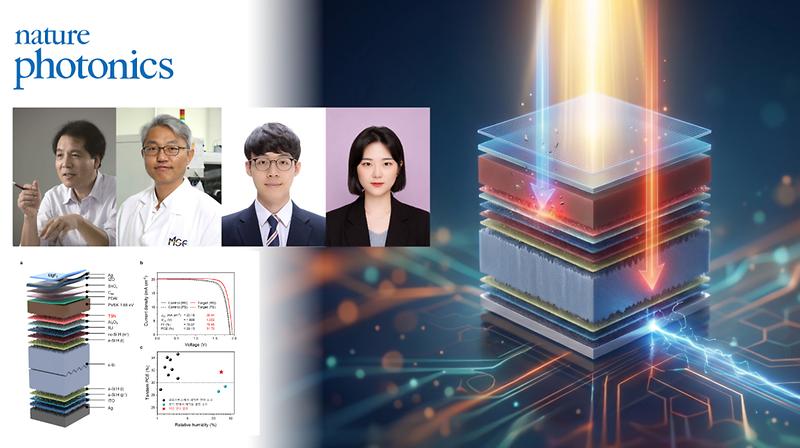
‘꿈의 태양전지’ 대량 생산 문턱 낮췄다!

페로브스카이트 태양전지 연구를 선도해온 UNIST 석상일 특훈교수 공동연구팀이 고효율 탠덤 태양전지의 대량생산에 필요한 계면 코팅 물질을 개발했다. 이 물질을 적용하면 수분과 산소에 노출되는 일반 공정을 통해서도 효율 30%가 넘어가는 페로브스카이트·실리콘 탠덤 태양전지를 만들 수 있게 됐다. 고효율 탠덤 전지 대량생산의 문턱을 낮춘 성과라는 평가가 나온다. 이번 연구는 광학·광자공학 분야의 세계적 학술지 네이처 포토닉스(Nature Photonics)에 6월 1일 공개됐다. UNIST 에너지화학공학과 석상일 특훈교수, 신소재공학과 최경진 교수팀은 사우디아라비아 KAUST 연구팀과 함께 3성분 물질을 이용한 전지 계면 코팅 물질을 개발했다고 11일 밝혔다. 페로브스카이트·실리콘 탠덤 태양전지는 페로브스카이트 전지와 실리콘 전지를 위아래로 쌓은 초고효율 전지다. 위쪽 페로브스카이트가 짧은 파장의 태양빛을 먼저 흡수하고, 아래쪽 실리콘이 남은 빛을 흡수해 기존 실리콘 태양전지보다 더 높은 효율을 낼 수 있다. 꿈의 태양전지로 불리며 중국을 비롯한 주요국이 주도권 확보 경쟁에 나선 이유다. 연구팀이 개발한 물질은 페로브스카이트층을 올리기 전, 전극 표면에 먼저 깔리는 얇은 접촉층이다. 이 층이 고르게 붙어 있어야 그 위에 바르는 페로브스카이트 용액도 균일하게 퍼지고, 전기 입자, 즉 전하가 사라지는 결함도 줄어든다. 기존에 쓰던 SAM 코팅층은 공기 중에 수분이 있으면 전극 위에 고르게 붙지 못하고, 페로브스카이트 용액을 바르는 과정에서도 쉽게 흐트러졌다. 고효율 전지는 수분과 산소를 차단한 특수 설비 안에서 만들어야 했고, 이는 대면적 생산 비용을 높이는 요인이 됐다. 연구팀의 3성분 물질은 기존 SAM 물질인 Me-4PACz 외에도 GDMA와 AG가 더 들어 있다. GDMA는 코팅층이 전극 위에 고르게 퍼지고 열처리 뒤 단단히 붙도록 돕고, AG는 페로브스카이트와 맞닿는 부분의 결함을 줄이는 역할을 한다. 결함이 줄어들면 빛을 받아 생긴 전하가 중간에 소실되지 않고, 그만큼 전하가 전극으로 더 잘 이동해 태양전지의 효율과 전압이 높아진다. 이 물질을 적용한 탠덤 전지는 일반 대기 중에서 만들었는데도 31.72%의 효율을 냈다. 이는 대기 중 제조 탠덤 전지 중 세계 최고 효율이다. 공인 인증 효율도 31.36%로 확인됐다. 내구성도 향상됐다. 겉을 감싸는 보호 포장 없이 85도의 뜨거운 공기 중에 600시간을 방치한 뒤에도 처음 성능의 92% 이상을 그대로 유지했으며, 실제 태양광을 모방한 강한 빛을 1,000시간 연속으로 쬔 후에도 90% 이상의 높은 효율을 지켜냈다. 이 물질은 페로브스카이트 전지 단독 제작 시에도 수율을 높일 수 있다. 7×7㎠ 대면적 기판에서도 페로브스카이트 박막이 고르게 만들어졌고, 불량률이 낮아졌다. 이번 연구는 UNIST의 김귀수 연구원, KAUST의 아디 프라세티오(Adi Prasetio) 연구원, UNIST의 노영임 연구원이 공동 제1저자로 참여했으며, UNIST 석상일 특훈교수, 최경진 교수, KAUST 스테판 드 울프(Stefaan De Wolf) 교수가 공동 교신저자로 참여했다. 홍콩중문대 선전캠퍼스, 독일 율리히 연구소 연구진도 함께 참여했다. 최경진 교수는 “정부의 ‘K-문샷 프로젝트’ 목표인 ‘초격차 초고효율 다중접합 태양전지’ 개발과 궤를 같이하는 연구”라며 “차세대 태양광 상용화에 크게 기여할 것으로 기대한다”고 말했다. 석상일 교수는 “고효율 탠덤 태양전지를 상용화하려면 성능뿐 아니라 실제 공정에서의 재현성과 생산 비용까지 함께 해결해야 한다”며 “이번 연구는 수분이 있는 일반 대기 중에서도 균일한 계면 박막과 높은 재현성을 확보할 수 있음을 보인 만큼, 대면적 제조 공정으로 확장하는 데 필요한 기술적 기반이 될 것”이라고 말했다. 이번 연구는 현대자동차, 과학기술정보통신부 한국연구재단(NRF), 기후에너지환경부 한국에너지기술평가원(KETEP) 등의 지원을 받아 이뤄졌다. (끝)

원자력공학과, ‘원자력 안전규제라운드테이블’ 개최

연구 2026년 06월 17일 수요일

수소 생산 촉매 전극, 국수 가락처럼 뽑아낸다!

물에서 수소를 생산하는 촉매 전극을 국수 가락 뽑듯 제조하는 기술이 새롭게 개발됐다. 내구성과 반응성이 뛰어난 섬유형 수소 생산 전극을 대량으로 생산할 수 있는 길이 열렸다. UNIST 신소재공학과 채한기 교수팀과 에너지화학공학과 백종범 교수팀은 킹압둘라과학기술대학교(KAUST) 자페르 야부즈(Cafer T. Yavuz) 교수팀과 공동으로 루테늄 촉매를 탄소섬유 안에 균일하게 넣은 섬유형 수소 생산 전극 제조 기술을 개발했다고 7일 밝혔다. 물을 분해해 수소를 얻는 수전해 장치의 전극은 보통 전기가 잘 통하는 기판 위에 촉매를 발라 만든다. 촉매를 바를 때 접착제를 섞게 되는데, 접착제가 촉매 표면을 가려 반응을 방해할 수 있다. 반면 탄소섬유를 얽어서 전극을 만들면 섬유 자체가 전도체 역할을 할 수 있고, 섬유 사이로 물과 전해질도 잘 드나들고, 생성물인 수소도 빠르게 빠져나갈 수 있다. 개발된 기술은 이러한 섬유에 촉매를 쉽게 넣어 전극을 대량 생산할 수 있는 기술이다. 섬유를 먼저 만든 뒤 촉매를 따로 입히는 방식이 아니라 촉매를 섬유 원료에 넣어 함께 뽑아내는 방식이다. 탄소섬유 원료인 고분자 용액과 루테늄 촉매 원료를 섞은 되직한 액체를 노즐로 밀어내 실처럼 뽑고, 이를 열처리해 만든다. 루테늄 성분이 이 과정에서 탄소 섬유 안팎에 작은 촉매 입자로 자리 잡게 된다. 관건은 루테늄 성분이 들어간 고분자 용액을 끊기지 않고 섬유로 뽑아내는 일이었다. 탄소섬유 원료 고분자에 금속 성분을 섞으면 쉽게 뭉치거나 용액이 굳어져, 작은 노즐로 길고 균일하게 뽑아내기 어렵다. 연구팀은 탄소섬유 원료 고분자와 루테늄 성분이 서로 적당히 붙도록 조절해, 촉매가 고르게 섞인 상태로 섬유를 뽑을 수 있는 조건을 찾아낼 수 있었다. 연구팀은 섬유 안에 있는 촉매가 표면에 더 드러날 수 있도록 산소 플라즈마 처리를 거쳐 전극을 완성했다. 완성된 전극을 수전해 장치에 적용한 실험 결과, 고전류 환경에서도 내구성이 뛰어났다. 전극은 500 mA cm⁻²의 높은 전류 조건에서 170시간 동안 계속 작동했으며, 수소 기체가 계속 발생하는 동안에도 전극 형태를 유지했다. 또 전극에 입혀진 촉매 자체의 성능을 평가하는 실험에서는 상용 백금 촉매보다 우수한 성능을 보였다. 이번 연구는 UNIST 이가현 박사, KAUST 김석진 연구교수가 제1저자로, UNIST 백인경 연구원이 공동 저자로 참여했다. 연구팀은 “이번 연구는 루테늄 촉매가 들어간 고분자 용액을 섬유로 뽑아내는 조건을 찾고, 금속 성분이 열처리 과정에서 나노입자로 자리 잡는 과정을 함께 규명했다는 데 의미가 있다”며 “실험실 수준에 머물던 섬유형 촉매 전극 제조를 대규모 롤투롤 연속 공정으로 확장할 수 있는 기반을 마련했다”고 설명했다. 채한기 교수는 “이번 기술은 금속 촉매를 탄소섬유 안에 균일하게 넣어 전극의 구조적 안정성을 높인 것이 특징”이라며 “수전해 전극뿐 아니라 안정성과 균일한 반응성이 중요한 다양한 촉매 분야로도 확장될 수 있을 것”이라고 말했다. 이번 연구는 과학기술정보통신부와 교육부가 지원하고 한국연구재단이 주관하는 중견연구자 지원사업(개인기초연구), 리더연구자지원사업(창의연구)을 통해 수행되었으며, 연구 성과는 미국화학회(ACS)가 발행하는 나노·소재 분야 최상위 국제 학술지인 '에이씨에스 나노(ACS Nano; Impact Factor: 16.1, Cite Score: 24.2)'에 5월 19일 출판됐다.

원자력공학과, ‘원자력 안전규제라운드테이블’ 개최

연구 2026년 05월 30일 토요일

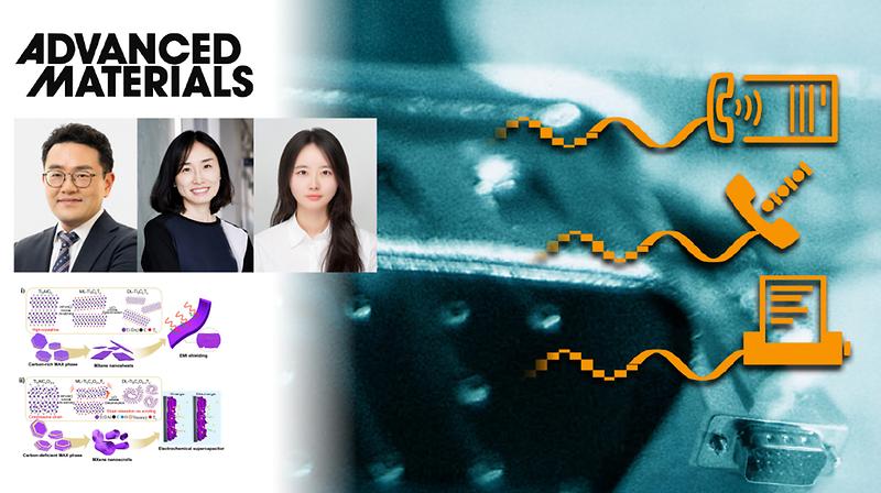
6G 통신과 배터리 잡을 ‘카멜레온 맥신’ 개발

* 본 보도자료는 한국연구재단 주관으로 작성되었습니다. (바로 가기) □ 국내 연구진이 탄소 조성 제어로 꿈의 신소재 ‘맥신(MXene)*’을 정밀 제어해 초고주파 EMI(Electromagnetic Interference Shielding) 차폐**와 고속 에너지 저장 성능을 세계적 수준으로 끌어올려 주목을 받고 있다. * 맥신(MXene) : 금속과 탄소층이 교대로 쌓인 2차원 나노소재로, 전기전도성이 뛰어나고 다양한 화합물 설계가 가능해 배터리·반도체·센서 분야의 꿈의 신소재로 불림. ** 초고주파 EMI(Electromagnetic Interference Shielding) 차폐 : 차세대 6G 통신, 고해상도 차량용 레이다, 위성 통신 등에서 발생하는 고주파 영역의 전자파 간섭을 막아내는 핵심 기술. □ 한국연구재단(이사장 홍원화)은 울산과학기술원 권순용·최은미 교수 연구팀이 MAX 전구체*의 탄소 조성을 정밀 제어해 맥신의 구조와 기능을 합성 단계에서 선택적으로 설계하는 데 성공했다고 밝혔다. * MAX 전구체 : 맥신을 만들기 위한 전 단계의 초기 원료 물질(화합물) □ 이번 연구성과는 과학기술정보통신부와 한국연구재단이 추진하는 나노․소재기술개발사업의 지원으로 수행됐으며, 재료과학 분야 세계적 권위지인 ‘어드밴스드 머티리얼즈(Advanced Materials)’에 5월 18일 게재됐다. □ 6G 통신, 자율주행 레이더, 고집적 패키징 등 차세대 전자기기가 고주파 환경으로 빠르게 전환됨에 따라, 전자파 간섭으로 인한 오동작을 막아줄 초박막 차폐 기술의 필요성이 커지고 있다. ○ 그러나 기존 금속계 차폐재는 높은 차폐성에도 불구하고 무겁고 부식에 취약해, 유연·경량·초박막화를 동시에 요구하는 차세대 전자기기에는 제약이 있었다. 이러한 이유로 높은 전도도와 용액공정 적합성을 갖는 맥신 계열 소재가 대안으로 주목받고 있다. □ 최근 맥신의 전기적·구조적 특성을 근본적으로 제어하기 위한 전구체 수준의 조성·구조 설계가 핵심 기술로 주목받고 있다. 연구팀은 맥스 전구체의 탄소 조성을 정밀 제어하는 방법으로 맥신의 구조와 기능을 선택적으로 구현하는 데 성공했다. ○ 탄소가 풍부한 조건에서는 전기전도도가 우수한 평면 나노시트 구조가 형성되어, 100GHz 초고주파 대역에서 탁월한 전자파 차폐 성능과 뛰어난 굽힘 내구성을 나타냈다. ○ 반대로 탄소가 부족한 조건에서는 나노 스크롤 구조가 자발적으로 형성되어 이온 이동 통로가 확장되었으며, 이를 통해 고용량과 압도적인 수명 특성을 가진 고속 에너지 저장 성능을 확보했다. ○ 연구팀은 이번 연구 성과를 통해 전구체 조성 조절만으로 차폐용 평면 시트와 에너지 저장용 스크롤 구조를 하나의 플랫폼에서 맞춤형으로 설계할 수 있음을 입증했다. □ 박재은(제1저자) 연구원은 “평면 시트는 전자파 차폐에, 나노스크롤은 에너지 저장에 유리하다는 점을 실험적으로 입증해 하나의 소재 플랫폼에서 응용 방향을 나눠 설계할 수 있게 됐다”고 밝혔다. ○ 그리고 권순용 교수는 "지난해에는 질소 치환으로 맥신의 전도도와 광대역 차폐 성능을 끌어올렸다면, 이번에는 전구체 조성만으로 맥신 구조 자체를 설계하는 단계로 나아갔다”며, “초박막이면서도 100GHz 대역에서 높은 차폐 성능과 굽힘 내구성을 함께 보여, 차세대 6G·레이다 환경에 필요한 유연 차폐 소재 가능성을 확인했다”고 밝혔다.

원자력공학과, ‘원자력 안전규제라운드테이블’ 개최

연구 2026년 05월 16일 토요일

"피부에 붙여 체온·기침·맥박까지 읽는다"... 온도·압력 감지 맥신 센서 개발

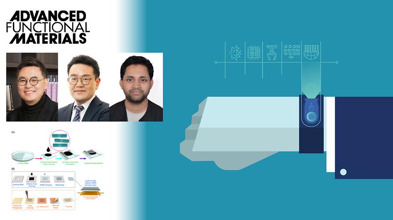
피부에 붙이면 체온뿐만 아니라 기침, 침 삼킴 등 미세한 신체 변화를 모두 읽어낼 수 있는 센서 소재가 새롭게 개발됐다. UNIST 반도체소재부품대학원 김수현·권순용 교수팀은 온도와 압력 변화를 모두감지할 수 있는 티타늄 탄질화물 기반의 초고민감도 맥신(MXene) 소재를 개발했다고 11일 밝혔다. 맥신은 금속과 탄소 또는 질소로 이루어진 원자층이 켜켜이 쌓여 있는 형태의 나노 물질이다. 두께가 매우 얇고 유연하면서도 전기가 잘 통해, 입는 컴퓨터나 웨어러블 헬스케어 기기에 들어가는 센서용 소재로 크게 주목받는 소재다. 연구팀이 이번에 개발한 맥신(Ti₃CNTz)은 질소가 없는 기존(Ti3C2Tx) 소재보다 온도 변화와 압력 자극에 대한 민감도가 각각 3배와 4배 이상 개선됐다. 아주 미세한 자극에도 전기저항이 크게 변한다는 뜻으로, 기계가 사람의 상태 등을 훨씬 더 선명한 전기신호로 인식할 수 있음을 의미한다. 연구팀은 최적의 질소 농도를 찾아내 이 같은 소재를 개발했다. 질소가 특정 영역에서 전자 밀도를 높이고, 격자 진동 현상을 강화해 외부 자극에 대한 반응성을 극대화한 덕분이다. 맥신의 아코디언 같은 구조는 기계적 강도도 강화하는 것으로 나타났다. 이러한 원리는 밀도함수이론(DFT) 계산과 방사광 기반 엑스선 흡수 미세 구조(XAFS) 실험 분석을 통해 입증됐다. 실험에서 이 소재를 이용해 만든 센서는 미세 압력 변화를 감지해 말하기, 침 삼키기, 기침하기 등 성대의 미세한 떨림을 완벽하게 구분해 냈다. 또한 눈가에서는 눈 깜박임을, 손목에서는 맥박 파형을 실시간으로 포착했으며, 신발 뒤꿈치에 부착해 보행 패턴을 분석할 수 있었다. 1~2mm 떨어진 상태에서 비접촉 온도 감지도 가능하다. 스마트폰 카메라 플래시에서 발생하는 적외선 열을 감지하거나, 손가락이 닿지 않은 상태에서도 접근만으로 온도 변화를 인식할 수 있었다. 제1저자인 데바난다 모하파트라(Debananda Mohapatra) 연구부교수는 “이번 2D MXene 연구는 지능형 센싱 분야의 새로운 기준을 제시한 성과”라며, “차세대 센싱 기기가 높은 감도와 우수한 확장성을 기반으로 인간-기계 인터페이스 구현에 기여할 수 있을 것으로 기대된다”고 설명했다. 또한 “이번 연구는 광범위한 2D MXene 나노소재 계열의 발전을 위한 발판이 되어 의료, AI 로봇, 스마트 웨어러블 등 다양한 분야에서 응용을 가속화할 것”이라고 덧붙였다. 김수현 교수는 “온도와 압력을 동시에 극도로 섬세하게 감지하면서도 신호 간 간섭을 효과적으로 제어할 수 있다는 점에서 차세대 인간-기계 인터페이스 및 지능형 로봇 전자 피부 기술의 전환점”이라며, “헬스케어뿐만 아니라 에너지 저장, 촉매, 전자기파 차폐 등 다양한 첨단 나노소재 분야로의 응용이 가능하다”고 강조했다. 김 교수는 이어 “그간 탄화물에 국한됐던 맥신 연구를 질소를 포함하는 탄질화물로 확장해 소재의 다양성을 확보했다는 점에서 큰 의미가 있다”라고 설명했다. 이번 연구 성과는 재료 과학 분야의 세계적 권위지인 '어드밴스드 펑셔널 머티리얼즈(Advanced Functional Materials)'에 4월 12일 온라인 공개됐다. 연구 수행은 과학기술정보통신부 한국연구재단(NRF)과 과학기술정보통신부의 이노코어(InnoCORE)사업의 지원으로 이뤄졌다.

원자력공학과, ‘원자력 안전규제라운드테이블’ 개최

연구 2026년 05월 14일 목요일

이산화탄소 제거하고 전기도 만드는 전기화학 전극 개발

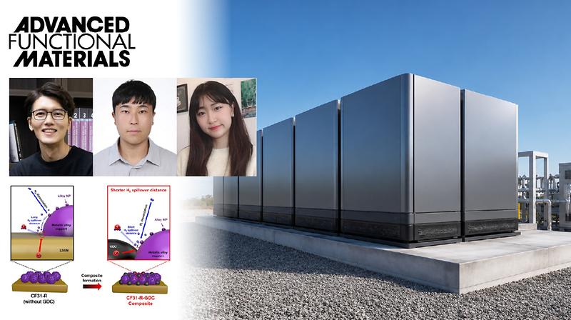
지구온난화의 주범인 이산화탄소를 유용한 물질로 바꿔주고, 수소로 전기도 만들 수 있는 장치의 성능과 수명을 획기적으로 개선하는 전극 물질이 개발됐다. UNIST 신소재공학과 조승호 교수팀은 POSTECH 안지환 교수, 서울대 한정우 교수, 중국 난징정보과학기술대학교 부윈페이 교수팀과 함께 이중층수산화물을 이용해 고온에서도 성능이 떨어지지 않는 고체산화물전지(SOC) 전극을 개발했다고 3일 밝혔다. 고체산화물전지는 수소나 메탄 같은 연료를 이용해 전기를 생산하는 장치다. 수소차의 연료전지와 달리 전기를 넣으면 반대로 반응을 돌릴 수 있어, 심야에 남는 전기로 다시 수소를 만들거나 온실가스인 이산화탄소를 분해해 산업용 가스인 일산화탄소를 만들 수도 있다는 장점이 있다. 연구팀이 개발한 전극은 지지체와 촉매 모두 금속으로 이뤄져 있어서 내구성이 뛰어나다. 기존 전극은 세라믹 지지체에 금속 촉매가 얹혀 있는 형태라, 세라믹과 금속 간의 구조 차이로 인해 600℃ 이상의 고온에서 장기 가동 시 금속 촉매가 뭉치거나 떨어져 나가는 문제가 있었다. 개발한 새로운 전극을 적용한 결과, 800℃에서 수소를 연료로 사용했을 때 기존 전극보다 약 1.5배 향상된 최대 출력(1.57 W/cm²)을 기록했다. 또 전기를 주입해 이산화탄소를 분해함으로써 일산화탄소를 생산하는 실험에서도 200시간 동안 안정적으로 작동하며 내구성을 입증했다. 지지체와 촉매 모두 금속인 전극을 만들 수 있었던 이유는 원료인 이중층수산화물 덕분이다. 이중층수산화물은 서로 다른 금속 이온이 한 층 안에 고르게 섞여 있고, 이 층이 겹겹이 쌓인 구조의 물질이다. 코발트와 철 이온이 섞인 이중층수산화물을 먼저 공기 중에서 한 번 가열해 지지체 역할을 할 금속 합금 뼈대를 굳힌 뒤, 이를 다시 수소를 넣어 가열하면 촉매 역할의 합금 나노 입자가 지지체 표면으로 솟아오르게(용출) 되는 원리다. 연구팀은 온도와 가열 환경별 이중층수산화물의 내부 구조(상변화)를 체계적으로 분석해 이 같은 물질을 합성해 낼 수 있었다. 또 첨가제(GDC)를 전극에 넣어 반응에 필요한 산소가 빠르게 공급되도록 했다. 공동연구팀은 “전극 교체를 줄여 장치 운영 비용을 낮춤으로써 고체산화물전지의 대중화에 기여할 수 있을 것”이라며 “수소와 전기 생산, 이산화탄소 업사이클링까지 연결되는 기반 기술”이라고 설명했다. 연구팀은 이어 “이중층수산화물은 그동안 저온 촉매나 배터리 전극 등에 주로 쓰이던 물질인데, 이번 연구에서는 이 물질이 고온에서 어떻게 변하는지를 분석해 고체산화물전지 전극으로 처음 적용했다는 점에서도 의미 있는 연구”라고 덧붙였다. 이번 연구에는 UNIST 에너지화학공학과 졸업생 김현민 연구원(現스탠포드대학교), UNIST 신소재공학과 졸업생 김윤서 연구원(現한국과학기술연구원) 그리고 서울대학교 재료공학부 서화경 연구원이 제1저자로 참여했다. 연구 성과는 재료 분야 글로벌 권위지인 ‘어드밴스드 펑셔널 머티리얼즈(Advanced Functional Materials)’에 4월 16일 출판됐으며, UNIST 이노코어 (InnoCORE) 프로그램과 한국연구재단의 지원을 받아 이뤄졌다.

원자력공학과, ‘원자력 안전규제라운드테이블’ 개최

Research 2026년 10월 01일 목요일

Beyond Ideal Conditions

《Editor's Note: Research works by controlling variables. But the problems it ultimately confronts rarely offer the same courtesy. Heat gets into storage tanks. Expertise shifts from one question to the next. Satellite images arrive out of season. Materials face conditions far beyond the laboratory norm. The obvious response is to restore control —keep the heat out, remove the variation, recreate the ideal test. But what happens when ideal conditions are no longer an option? This month, UNIST researchers took that question in different directions. Some intervene before a problem takes hold —or after a familiar line of defense has failed. Others design for rather variation than uniformity, or put promising results to more demanding tests. The approaches differ, but the underlying shift is the same —rather than trying to restore control, they rethink the solution around what actually changes.》 CHANGE WHERE YOU INTERVENE “Sometimes the best place to solve a problem is not where it appears.” For atomically thin semiconductors, contamination during fabrication can be especially difficult to undo. Plasma exposure changes the chemistry of photoresist, causing residue to bind more strongly to MoS₂. Aggressive cleaning, meanwhile, risks damaging the material itself. Rather than trying to remove the residue afterward, UNIST researchers placed a removable, 5-nanometer metal layer over the semiconductor before patterning, preventing the contamination from reaching its surface. The resulting transistors showed roughly a tenfold reduction in contact resistance and a similar increase in on-current. Liquid hydrogen presents the problem from the opposite direction. Even well-insulated tanks cannot keep heat out indefinitely. Instead of treating insulation as the only line of defense, researchers investigated whether metal-organic frameworks could capture evaporating hydrogen after heat enters the tank and slow the buildup of pressure. In modeling, IRMOF-20 preserved about 97 percent of the volumetric capacity of liquid hydrogen while extending the projected storage period from roughly 64 to 221 days. One solution acts before the problem reaches the material: the other takes effect after a familiar line of defense has been breached. In both cases, changing where researchers intervene changes what can be done about the problem. ■ New Process Shields 2D Semiconductors from Fabrication Residue (Small) ■ Rethinking Liquid Hydrogen Storage with MOFs (Nature Communications) WORK WITH WHAT CHANGES “When the world refuses to stay consistent, the method has to change with it.” Personalization gets harder when expertise refuses to stay fixed. A person who is an expert in one subject may be a novice in another—and even within the same field, expertise can change from question to question. ExPerT responds to that variation rather than smoothing it away. By combining the semantics of each query with patterns in a user's typing behavior, the framework estimates expertise for individual questions and adjusts the detail, terminology, and complexity of its answers accordingly. In a study involving 40 participants and 1,270 queries, it reduced expertise-estimation error by 65.7 percent compared with the strongest baseline. For wildfire assessment, the changing conditions are not the user but the landscape. Satellite images taken before and after a fire may come from different seasons, allowing natural changes in vegetation to be mistaken for fire damage. Instead of requiring seasonally matched images, UNIST researchers use nearby unburned vegetation to estimate seasonal change and correct the comparison. Across 12 US wildfires, it achieved a correlation of 0.72 with field observations using seasonally mismatched imagery—nearly matching the 0.73 obtained with images from similar seasons. One method adapts to knowledge that changes from question to question—the other accounts for landscapes that change with the season. Neither requires the variation to disappear before the analysis can begin. ■ AI Personalization Adapts Answers to What Users Know (ACL '26) ■ Assessing Wildfire Burn Severity Across Seasons (Remote Sens. Environ.) TEST WHAT HOLDS UP “A promising result means more when it holds up under a more demanding test.” Perovskite solar cells (PSCs) have reached impressive efficiencies, but performance under controlled conditions tells only part of the story. UNIST researchers developed a molecular interface that delivered a certified power-conversion efficiency of 26.37 percent, then subjected the cells to repeated swings between −100°C and +100°C. After 16 cycles, they retained about 91 percent of their initial efficiency—putting their stability to a far more demanding test. AI highlight detection faces a different gap between promising results and meaningful tests. Existing benchmarks have largely relied on videos lasting only a few minutes, even though real sports broadcasts can run for hours. SVHighlights closes the gap with 320 videos across eight sports and 640.18 hours of footage. Its videos average about two hours—roughly 30 to 60 times longer than those in existing datasets—allowing AI models to be evaluated under conditions much closer to the task they are meant to perform. One study subjects a material to extreme temperature swings, while the other tests AI against the scale of the task it is meant to perform. Both ask the same question: Does a promising result still hold when the test starts to resemble the challenge it is meant to meet? ■ PSCs Hold Up Under Extreme Temperature Swings (Joule) ■ AI Sports Highlight Detection to a More Realistic Test (ACM KDD '26) Explore the latest issue and follow 『The UNIST Brief』 on LinkedIn to stay updated. Subscribe via LinkedIn

원자력공학과, ‘원자력 안전규제라운드테이블’ 개최

News 2026년 09월 29일 화요일

Successful Completion of 2026 SEMI Research Day

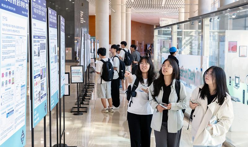
UNIST held its inaugural 2026 UNIST SEMI Research Day on September 21–22, bringing together undergraduate and graduate students to share research and explore work across the university’s semiconductor community. The two-day event featured 14 semiconductor laboratories and 31 student research posters, alongside networking and interactive programs designed to encourage exchange across research groups and disciplines. At the SEMI LAB SHOWCASE, participating laboratories presented their research areas and current work, giving students an opportunity to explore research beyond their own fields. The poster session featured 14 undergraduate projects from the Department of Semiconductor Engineering and the interdisciplinary semiconductor program, along with 17 graduate projects in semiconductor materials and components. Students presented their work to fellow researchers and other members of the UNIST community, with outstanding projects selected separately in undergraduate and graduate categories. Interactive programs complemented the research sessions, including a Networking Zone and activities that encouraged participants to visit laboratory exhibits and student posters. A semiconductor-themed keycap workshop provided a more informal setting for students to connect. “We hope Research Day gives students an opportunity to experience the breadth of semiconductor research at UNIST, understand one another’s work, and discover new areas of interest,” said Soo-Hyun Kim, Head of the Department of Semiconductor Engineering. “We will continue to expand exchange across laboratories and disciplines and develop the event as a forum for UNIST’s semiconductor research community.” The event was jointly organized by the Department of Semiconductor Engineering and UNIST semiconductor education programs supported by the Ministry of Trade, Industry and Energy and the Ministry of Education.

원자력공학과, ‘원자력 안전규제라운드테이블’ 개최

Research 2026년 09월 28일 월요일

Stretchable QLEDs Bring High-Resolution Displays Closer to Soft Electronics

A research team, affiliated with UNIST has developed intrinsically stretchable quantum-dot light-emitting diodes (QLEDs) that combine high brightness, fine pixel patterning, and mechanical stretchability in a single device platform. Led by Professor Moon Kee Choi of the Department of Materials Science and Engineering at UNIST, the team worked with Professor Jiwoong Yang's team at DGIST and Associate Director Dae-Hyeong Kim of the IBS Center for Nanoparticle Research to develop a fabrication strategy known as LIFT—ligand engineering at the interface and intaglio film transfer printing. The method enabled stretchable light-emitting layers to be patterned at high resolution while preserving the electrical and mechanical properties needed for high-performance devices. Stretchable displays are being explored for wearable electronics, electronic skin, and soft robotics, where conventional rigid displays cannot readily conform to moving or irregular surfaces. Many existing designs accommodate stretching by allowing the connections between pixels to deform while the light-emitting pixels themselves remain relatively rigid. As the display expands, this can reduce the proportion of the surface that actively emits light. Making the emissive material itself stretchable could overcome this limitation, but it introduces a different set of problems. Soft, elastomeric materials are difficult to pattern into sharply defined microscopic pixels, while the polymers that provide stretchability can interfere with charge transport and reduce light-emitting efficiency. The researchers addressed both problems by engineering the surface of a quantum-dot nanocomposite. They selectively replaced polymer-rich regions at the surface with short, polar ligands, creating a nanoscale interface that lowers the barrier to hole injection while preserving the mechanical compliance of the underlying material. They paired this interface engineering with a thermally assisted transfer-printing process. Applying heat during printing concentrates mechanical strain along the boundaries of each pattern, allowing the soft emissive film to separate cleanly and form sharply defined pixels rather than stretching or tearing during transfer. Using the process, the team patterned quantum-dot emissive layers at resolutions of up to 16,000 pixels per inch (PPI) and produced red, green, and blue stretchable patterns. The researchers also demonstrated a 12 × 12 multicolor passive-matrix display, showing that the technique could be extended beyond individual pixels to an addressable display architecture. The fully stretchable QLEDs remained functional at strains exceeding 65% and reached a maximum luminance of 53,300 cd m⁻², with an external quantum efficiency of 8.0%. In conventional device architectures, the engineered emissive layers achieved an external quantum efficiency of up to 23.9%. “This work provides a way to improve both the performance and resolution of intrinsically stretchable displays,” said Professor Choi. “The approach could help advance soft optoelectronic systems that require light-emitting devices to conform closely to the human body or other deformable surfaces.” Supported by programs of the Ministry of Science and ICT (MSIT) and the National Research Foundation of Korea (NRF), including the Mid-Career Researcher Program and the Nano & Materials Technology Development Program, the study was published online in Nature Nanotechnology on September 14, 2026. Journal Reference Jisu Yoo, Kyunghoon Lee, Ji Su Kim, et al ., “High-resolution intrinsically stretchable quantum-dot displays through thermally assisted intaglio transfer printing,” Nat. Nanotechnol., , (2026).

원자력공학과, ‘원자력 안전규제라운드테이블’ 개최

Research 2026년 09월 08일 화요일

Perovskite Solar Cells Hold Up Under Extreme Temperature Swings

Summary The advent of self-assembled monolayer (SAM)-based hole-selective layers (HSLs) has revolutionized inverted perovskite solar cells (i-PSCs) by enabling record efficiencies, but they are constrained by incomplete surface coverage and interfacial heterogeneity. We devise topology-governed SAMs featuring isomeric linker patterns (LY-ortho [o], LY-meta [m], and LY-para [p]) and uncover the principle that conformational ordering dictates surface coverage and interfacial interaction coupling with perovskite. The topology-optimized LY-m forms a homogeneously dense, stable HSL with superior energy alignment and interfacial passivation. Devices incorporating LY-m achieve a record-high open-circuit voltage of 1.231 V, accompanied by an efficiency of 26.39% (certified 26.37%), while maintaining robust operational stability and scalability. Beyond laboratory metrics, LY-m-based devices withstand −100°C to 100°C thermal cycling with only ∼9% loss, far exceeding the operational limits of state-of-the-art commercial SAMs, while maintaining over 80% of their initial performance at 85°C (T80 ≅ 2,000 h). This work resolves the long-standing role of linker topology and paves the way for extreme-environment-resilient and scalable perovskite photovoltaics. Temperature swings are a major challenge for perovskite solar cells (PSCs), particularly in environments such as space, where materials may repeatedly move between extreme cold and heat. Led by Professors Changduk Yang and Seungjae Shin of the Department of Energy and Chemical Engineering and Professor Myung Hoon Song of the Department of Materials Science and Engineering at UNIST, the team developed perovskite solar cells that withstand such extremes by stabilizing a critical molecular interface. The cells retained about 91% of their initial efficiency after cycling between −100°C and +100°C, with a certified power-conversion efficiency of 26.37%. The key to this advancement is a self-assembled monolayer (SAM), a molecule-thin layer that helps move electrical charges between the electrode and the perovskite absorber. Under severe thermal stress, SAM molecules can shift or cluster, disrupting the interface and degrading performance. The team addressed this problem by changing where the molecular components of the SAM connect. They synthesized three versions with different linker positions and found that LY-m adopted a tilted orientation, allowing its molecules to pack densely and uniformly on the electrode. This arrangement also suppresses the molecular reorganization that can occur under large temperature swings. In thermal-cycling tests, LY-m cells were held alternately at −100°C and +100°C for 30 minutes at each temperature over 16 cycles. They remained operational with only about a 9% loss in efficiency, while cells using a commercial SAM failed under the same conditions. LY-m cells also reached a peak efficiency of 26.39%, with a certified efficiency of 26.37% and an open-circuit voltage of 1.231 V. At 85°C, they maintained more than 80% of their initial performance for approximately 2,000 hours. The approach also performed well at larger scales: a 1 cm² cell achieved 23.25% efficiency, while a 3 × 1 cm² mini-module reached 21.20%. “By changing only the position of the molecular connection, we were able to control how the molecules pack on the electrode,” said Professor Yang. “The resulting interface combines high efficiency with thermal stability, offering a promising route toward perovskite photovoltaics for environments with extreme temperature variations.” The study has been participated by Seunglok Lee and Jeewon Park of the Department of Energy and Chemical Engineering and Jingyu Yang of the Department of Materials Science and Engineering at UNIST, as co-first authors of the study. Published in Joule on August 3, the study has been supported by the Nano & Material Technology Development Program through the National Research Foundation (NRF) of Korea and the InnoCORE program of the Ministry of Science and ICT (MSIT). Journal Reference Seunglok Lee, Jinkyu Yang, Jeewon Park, et al., "Topology-governed self-assembled monolayers enable perovskite solar cells stable at −100°C to +100°C," Joule , (2026).

원자력공학과, ‘원자력 안전규제라운드테이블’ 개최

Research 2026년 09월 03일 목요일

Reducing Charge Loss in Organic Photoanodes for Solar Water Splitting

Abstract Organic photoelectrochemical (PEC) cells for solar water splitting typically utilize bulk heterojunction (BHJ) structures to circumvent the intrinsically short exciton diffusion lengths of organic semiconductors. However, stochastic donor/acceptor networks in BHJs often result in disordered interfacial contacts, leading to severe charge recombination. Herein, we report a pseudo-bilayer (PS-Bi) organic photoanode featuring a vertically ordered donor–acceptor configuration established via sequential deposition. Our systematic investigation reveals that this PS-Bi structure promotes selective charge transport and suppresses recombination due to its high domain purity, thereby facilitating efficient charge transfer at the interface. Consequently, the optimized PS-Bi photoanodes deliver an enhanced average photocurrent density (Jph) of 1.75 ± 0.03 mA cm−2 at 1.23 V versus the reversible hydrogen electrode for solar water oxidation, while simultaneously exhibiting a significant cathodic onset shift and extended operational stability compared to their BHJ counterparts (Jph = 1.44 ± 0.07 mA cm−2). This study demonstrates that employing the PS-Bi structure is a promising strategy for achieving high-performance and stable organic PEC systems for sustainable solar fuel production. Producing hydrogen from sunlight depends in part on how efficiently a photoelectrode can separate and move electrical charges. In organic photoelectrodes, however, the conventional practice of mixing semiconductor materials can create disordered pathways that allow those charges to recombine, reducing both performance and stability. A research team, led by Professors Han Hee Cho, Moon Kee Choi, and Myung Hoon Song of the Department of Materials Science and Engineering at UNIST, working with researchers at École Polytechnique Fédérale de Lausanne (EPFL), has developed an organic photoanode with a more ordered internal structure. The new design improved photocurrent by about 22% while extending operational stability. The team created what is known as a pseudo-bilayer (PS-Bi) structure by depositing two organic semiconductor materials in sequence. As the second layer is applied, it partially penetrates the first, forming a mixed region at the interface while preserving more distinct layers above and below. Conventional organic photoelectrodes typically use a bulk heterojunction (BHJ), in which donor and acceptor materials are mixed throughout the film. This arrangement helps generate and separate charges, but its irregular internal pathways can also bring electrons and holes back together before they contribute to the chemical reaction. The PS-Bi combines the advantages of both approaches. Charges are generated and separated in the mixed region, while the more ordered layers guide electrons and holes in different directions. This reduces recombination and allows more of the generated charge to drive water oxidation. In tests, the PS-Bi photoanodes achieved an average photocurrent density of 1.75 mA cm⁻², compared with 1.44 mA cm⁻² for conventional BHJ photoanodes, an increase of about 22%. The voltage required to initiate water oxidation also fell from 0.35 V to 0.15 V, allowing the reaction to begin with less external electrical input. The structural change also improved durability. Based on the time required for photocurrent density to fall to 0.5 mA cm⁻², the pseudo-bilayer photoanodes remained operational substantially longer than their BHJ counterparts. The researchers also found that the two structures degrade differently. In BHJ photoanodes, highly reactive holes can damage the organic semiconductor within the intermixed structure. The more ordered pseudo-bilayer reduces damage within the donor–acceptor region, helping the photoanode maintain its performance for longer. “Conventional organic photoelectrodes mix donor and acceptor materials throughout the film, which can lead to charge losses and faster degradation,” said Professor Cho. “By controlling how the two materials are arranged, we were able to improve both charge transport and operational stability.” He further added, “The lower operating voltage could also help in the development of systems that ultimately produce hydrogen using sunlight without an external electrical bias.” The study was published online in Chemical Engineering Journal on July 16, 2026. The research was supported by the National Research Foundation of Korea (NRF), funded by the Ministry of Science and ICT (MSIT), and the InnoCORE program. Journal Reference Gyu Won Chae, Seong Rae Kang, Jin Su Park, et al. , “A pseudo-bilayer organic photoanode for solar water oxidation,” Chem. Eng. J., (2026).

원자력공학과, ‘원자력 안전규제라운드테이블’ 개최

Research 2026년 09월 02일 수요일

New Process Shields 2D Semiconductors from Fabrication Residue

Abstract Achieving the theoretical performance of 2D molybdenum disulfide (MoS2) electronics is currently bottlenecked by interfacial contamination derived from lithographic processing. A critical, yet often overlooked, mechanism is the interaction between photoresist (PR) and plasma, which chemically alters the interface. In this work, we elucidate the atomistic origin of this degradation: theoretical calculations based on molecular dynamics (MD) and density functional theory (DFT) reveal that plasma exposure functionalizes the PR with oxygen, drastically increasing its adsorption energy on the MoS2 surface from −1.15 to −2.36 eV. This doubling of adsorption energy creates thermodynamically stable, hardened residues that resist conventional removal methods. To overcome this fundamental limitation, we introduce a universal prevention-first strategy: Sacrificial Metal Mask Lithography. By utilizing a sacrificial layer to physically isolate the channel, we shield the MoS2 from reactive plasma species, preventing the formation of hardened residue entirely. This strategy results in a ten-fold reduction in contact resistance (RC) from 2.59 × 10⁶ Ω·µm to 2.58 × 10⁵ Ω·µm and an order-of-magnitude enhancement in on-current. Crucially, we demonstrate the universality of this method by successfully applying it to top-gated transistor arrays, electron-beam lithography (EBL), and atomic layer deposition (ALD)-synthesized films. Two-dimensional (2D) semiconductors, such as molybdenum disulfide (MoS2) hold promise for smaller, thinner electronics, but their extreme thinness also makes them particularly vulnerable to contamination during fabrication. Even small amounts of residue can interfere with electrical performance. A research team, led by Professor Myung-Soo Kim of the Department of Electrical Engineering and Professor Byoung Jo Kim of the Graduate School of Semiconductor Materials and Devices Engineering at UNIST, has developed a fabrication method that protects MoS2 from photoresist (PR) residue. The approach uses a thin, removable metal layer to keep the residue from reaching the semiconductor surface. PR is a light-sensitive material used to pattern circuits during semiconductor fabrication. When exposed to plasma, however, it can leave residue on MoS2 that conventional solvents struggle to remove. More aggressive cleaning can damage or even detach the atomically thin material from its substrate. Rather than removing the residue after it forms, the researchers prevent it from reaching the MoS2 in the first place. They place a 5-nanometer-thick metal layer over the semiconductor before patterning. Once fabrication is complete, the metal is dissolved, carrying the accumulated residue with it. Transistors made with the new process had a contact resistance of 2.58 × 10⁵ Ω·μm, about one-tenth that of devices made conventionally. Their on-current, or the current flowing when the transistor is switched on, increased by roughly tenfold. The researchers also found no clear damage to the crystal structure of MoS2 after the metal layer was removed. The team also uncovered why the residue is so difficult to remove. Molecular-level calculations showed that plasma exposure introduces oxygen into the PR, changing its chemistry and causing it to bind much more strongly to MoS2. The calculated adsorption energy shifted from −1.15 to −2.36 eV, roughly doubling the strength of the interaction. “This process can be used not only with conventional semiconductor patterning, but also with electron-beam lithography for finer features,” said Dahyun Kim, first author of the study. “We also found that it works with MoS2 produced by different synthesis methods.” The researchers tested the method with top-gated transistor arrays, electron-beam lithography, and MoS2 films grown by atomic layer deposition, showing that it can be used across different device structures and fabrication methods. “MoS2 is a promising material for making semiconductor devices, such as transistors smaller and thinner,” said Professor Myung-Soo Kim. “By addressing process contamination that has limited device performance, this work could help advance highly integrated logic and memory devices based on 2D semiconductors.” The study was published online in Small on August 11, 2026. The research was supported by the Ministry of Science and ICT (MSIT), National Research Foundation of Korea (NRF), Institute of Information & Communications Technology Planning & Evaluation (IITP), InnoCORE program, Ministry of Trade, Industry and Energy (MOTIE), and Korea Institute for Advancement of Technology (KIAT). Journal Reference Dahyeon Kim, Yanfeng Zhao, Sungyeon Kim, et al ., “Preventing Plasma-Induced Resist Hardening in Molybdenum Disulfide Transistors via Sacrificial Metal Mask Lithography,” Small, (2026).

원자력공학과, ‘원자력 안전규제라운드테이블’ 개최

Research 2026년 09월 01일 화요일

Rethinking What Matters

《Editor's Note: What does it take to make something work better? The answer may be to pare back what is unnecessary, rethink how existing parts are arranged, find another route around a constraint, or widen the frame of the problem itself. This month's UNIST research offers answers in many forms—from leaner AI systems and redesigned material structures to an unexpected route for electron transfer and a broader view of cancer drug resistance. Some of those answers run counter to what we might expect. 》 Less Can Be Enough “How much does AI really need?” AI has spent years scaling up. But recent UNIST research asks a different question—how much can be taken away while keeping what matters? At ACL 2026, researchers introduced GMoE, an architecture that shares experts across layers rather than repeatedly storing similar ones. It cut model parameters by about 63 percent, from 549 million to 204 million, while average accuracy remained virtually unchanged—39.51 percent, compared with 39.55 percent for the baseline. The next target was data. Presented at ICML 2026, CSOR removes redundant training images while preserving meaningful variation within each identity. Using roughly half the original dataset, models retained more than 95 percent of full-data performance in re-identification (ReID) tasks. A third study moved to hardware. An automated design framework for logic-in-memory (LiM) computing optimized the placement and routing of computing elements, cutting computation cycles by 19.6 percent under area constraints. ■ GMoE—Expert Sharing for Smaller AI Models (ACL 2026) ■ CSOR—Less Training Data for ReID AI (ICML 2026 ) ■ LiM—Smarter Chip Design (IEEE TCAD) Arrangement Matters “In materials, where can matter as much as what.” More iron, less corrosion. Iron (Fe) is one of magnesium's most damaging impurities, yet UNIST researchers produced a Mg alloy containing more than six times as much Fe as ultra-high-purity Mg—and it still corroded more slowly. Instead of removing the impurity, the team added scandium (Sc) to form core–shell particles that isolate Fe-rich regions from the surrounding Mg. The corrosion rate fell from 22.2 to 0.38 millimeters per year, nearly a 60-fold reduction. At the molecular scale, thermal annealing changed the packing of an organic semiconductor, more than tripling its absorption dissymmetry and even reversing its preferred handedness of circularly polarized light (CPL). The resulting near-infrared (NIR) photodetector achieved a dissymmetry factor of 0.1 at 850 nanometers. The scale shifts again in perovskite solar cells (PSCs). The same high-efficiency formulation crystallized differently depending on the buried interface beneath it. Tailoring the chloride chemistry to the inverted architecture produced a device with 26.3 percent efficiency and a fill factor (FF) of up to 86.8 percent. ■ Mg Alloy—Shielding Fe to Slow Corrosion (Science Advances) ■ NIR Photodetector—Turning Molecular Packing (Advanced Science) ■ PSCs—Why Architecture Changes Performance (Joule) Another Way Through “How spin opens a new route for electron transfer.” Conventional energetics suggested that electron transfer should be unfavorable. Yet in manganese (Mn)-doped quantum dots (QDs), spin-exchange interactions enabled transfer more than ten times faster than in undoped QDs. The mechanism could help capture energetic hot electrons before their excess energy dissipates—a longstanding challenge in photocatalysis and solar-energy conversion. ■ Hot Electrons—Spin-Enabled Transfer (Nature Communications) Beyond the Tumor “The cells helping cancer resist treatment.” Some of the cells helping breast cancer resist treatment are not part of the tumor at all. UNIST researchers found that nearby fat cells can become cancer-associated adipocytes, which release complement factor D and activate survival signaling in cancer cells. In mouse models, disrupting this TRAP1-driven communication improved the response to chemotherapy, pointing to surrounding adipocytes as potential therapeutic targets alongside the tumor itself. ■ Breast Cancer—How Nearby Fat Cells Drive Drug Resistance (STTT) Explore the latest issue and follow 『The UNIST Brief』 on LinkedIn to stay updated. Subscribe via LinkedIn

원자력공학과, ‘원자력 안전규제라운드테이블’ 개최

Research 2026년 08월 28일 금요일

New X-Ray Mapping Technique Enables Non-Destructive Analysis of Large-Area Perovskite Solar Cells

Abstract Scaling perovskite solar cells (PSCs) into large-area modules requires precise control of structural uniformity and mechanical integrity. However, scalable deposition often introduces mesoscale heterogeneities, including grain-orientation disorder and lattice-strain gradients, which limit efficiency and stability. Here, we report an intact-film orthogonal two-dimensional X-ray diffraction mapping (2DXDM) technique that enables full-field, quantitative crystallographic analysis of large-area perovskite films without physical sectioning. The method resolves spatial variations in crystallinity, orientation coherence, and lattice strain across complete modules and is validated against conventional sectioned analyzes such as grazing-incidence wide-angle X-ray diffraction (GI-WAXD) and X-ray diffraction (XRD). Using this approach, we compare static spin-coating (SSC) and dynamic spin-casting (DSC). DSC yields more homogeneous films with relaxed lattice stress and controlled solvate evolution, thereby reducing edge defects. As a result, DSC-based modules achieve 23.0% efficiency (22.7% certified) over 86.4 cm2 and retain over 80% of their initial efficiency after 1,000 h of operation. Perovskite solar cells (PSCs) have reached impressive efficiencies at laboratory scale, but maintaining that performance in larger modules remains challenging. As the films grow larger, differences in crystal orientation and internal strain can develop across the surface, creating defects that reduce efficiency and long-term stability. A research team led by Professors Dong-Seok Kim and Jin Young Kim of the School of Energy and Chemical Engineering and Professor Tae Joo Shin of the Graduate School of Semiconductor Materials and Devices Engineering at UNIST, together with Dr. Yun Seop Shin of the Korea Research Institute of Chemical Technology (KRICT), has developed an X-ray technique that maps these structural variations across an intact perovskite film. Called two-dimensional X-ray diffraction mapping (2DXDM), the technique shows how crystallinity, crystal orientation, and residual strain vary across an entity film without damaging it. Conventional methods often examine selected regions, provide averaged measurements, or require samples to be cut into sections. PSCs are made by depositing a liquid precursor onto a surface, where it dries and crystallizes into a light-absorbing layer. Across a large area, differences in drying and crystallization can leave the center and edges with different structural properties. The researchers used 2DXDM to compare two methods for forming large-area films. In static spin-coating (SSC), the precursor solution is applied before the substrate is spun, while dynamic spin-casting (DSC) deposits the solution drop by drop as the substrate rotates. The resulting maps showed that DSC produced more homogeneous films, with more consistent crystal orientation and lower residual strain. Additional X-ray measurements linked this improvement to better control over colon drying and crystal formation, which helped reduce structural defects near the edges. The more uniform films also delivered strong performance at module scale. DSC-based modules reached a power conversion efficiency of 23.0% over an active area of 86.4 cm², with a certified efficiency of 22.7%. Encapsulated modules retained more than 80% of their initial efficiency after 1,000 hours under continuous illumination. “Conventional methods make it difficult to see how structure varies across an entire film, and cutting a sample for analysis can alter the strain already present” said Professor Shin. “With 2DXDM, we can examine the full area without damaging the film and identify where structural differences occur.” Professor Dong-Seok Kim added, “For large-area perovskite films, what matters is structural uniformity across the entire surface, not just at a few individual points. By showing how fabrication conditions affect that uniformity, this approach can help guide the development of more efficient large-area modules.” Dong Shin Kim of the Graduate School of Semiconductor Materials and Devices Engineering and Jae Hwi Lee of the School of Energy and Chemical Engineering at UNIST, served as first authors. The research used the UNIST-PAL 6D beamline at the Pohang Accelerator Laboratory. The findings were published online in Joule on July 23, 2026. The research was supported by the Ministry of Science and ICT (MSIT), Ministry of Education (ME), National Research Foundation of Korea (NRF), Ministry of Trade, Industry and Energy (MOTIE), Korea Institute of Energy Technology Evaluation and Planning (KETEP), Korea Institute for Advancement of Technology (KIAT), and Korea Research Institute of Chemical Technology (KRICT). Journal Reference Dongshin Kim, Jaehwi Lee, Dongmin Lee, et al ., “Intact-film orthogonal 2D X-ray diffraction mapping for crystallographic homogeneity evaluation in perovskite solar modules,” Joule , (2026).

원자력공학과, ‘원자력 안전규제라운드테이블’ 개최

News 2026년 08월 26일 수요일

UNIST Opens Nexus Hall, Connecting Engineering Education with Industry

Students at UNIST will have a new space to learn with advanced technologies—and closer to the industry expertise behind them. Nexus Hall, newly opened in the College of Engineering, brings a wall-sized LED display and integrated audiovisual systems to courses and programs spanning semiconductors, materials, and engineering. Developed with support from Ulsan Metropolitan City, the hall replaces a conventional projector-based classroom into a digital teaching environment built around the large LED display. An electronic lectern and instructor-tracking cameras complete the setup, while the classroom itself has been redesigned for better visibility and comfort. The name Nexus , meaning a point of connection, captures the idea behind the space—bringing education and research into closer contact with industry. The hall will host regular and special courses, along with interdisciplinary semiconductor courses that bring perspectives from outside the university into the classroom. That connection was already evident at the opening ceremony on August 25, 2026. Joo-Young Lee, Executive Vice President of Samsung Electronics, and Se-Yeon Kim, Executive Vice President of SK hynix, spoke with students about shifts in the semiconductor industry, emerging technologies, and the expertise the field increasingly demands. About 80 representatives from UNIST, Ulsan Metropolitan City, and industry attended the opening, including UNIST President Chong Rae Park and Ulsan Mayor Sang-Wook Kim. The new hall also reflects a broader effort by UNIST and Ulsan Metropolitan City to connect education and research with the region's industrial base. UNIST plans to expand ties with semiconductor companies and research institutions, drawing on UNIST's research strengths and Ulsan's manufacturing expertise as the region moves toward more AI-enabled industry. “Nexus Hall will bring education, research, and industry closer together as we prepare students for rapidly changing industries,” said UNIST President Chong Rae Park. “By connecting academic training more closely with industry, we hope to develop students who can work across disciplines and contribute to industrial innovation in Ulsan.” “Semiconductors underpin advances in artificial intelligence (AI), batteries, future mobility, and other emerging industries,” said Ulsan Mayor Sang Wook Kim. “We will continue working with UNIST and other universities in the region to develop the expertise companies need and create more opportunities for young people to build their careers in Ulsan.”

원자력공학과, ‘원자력 안전규제라운드테이블’ 개최

Research 2026년 08월 25일 화요일

New Strategy Shields Magnesium from Impurity-Driven Corrosion

Abstract Magnesium (Mg) alloys offer high weight-saving potential for transportation technologies; However, their use remains constrained by poor corrosion resistance, which is strongly dependent on alloy purity. The presence of impurities, such as iron (Fe), severely degrades the corrosion resistance of Mg alloys. Herein, we present an alloy design strategy that substantially improves the corrosion resistance, even when using low-purity Mg. Our method produces core-shell particles, where an Fe-rich core is encapsulated by an Fe-depleted shell embedded in the Mg matrix. This shell acts as a local microscavenger that isolates the core and suppresses impurity-triggered corrosion, resulting in corrosion resistance achievable only when using ultrahigh-purity Mg. This approach provides a practical pathway for the development of high-performance Mg alloys without relying on costly purification. Magnesium (Mg) is prized for its exceptionally low weight, but its tendency to corrode has limited its wider use in cars, aircraft, drones, and other applications where lighter materials could offer significant advantages. Even trace amounts of iron (Fe) can accelerate that corrosion, making material purity a critical—and costly—part of producing durable Mg alloys. Professor Sung Soo Park and his research team in the Department of Materials Science and Engineering at UNIST approached the problem differently. Rather than removing Fe impurities, they designed the alloy to isolate them and limit their ability to trigger corrosion. The resulting material encloses Fe-rich regions within specially formed particles and maintains strong corrosion resistance despite being made from lower-purity Mg. The researchers achieved this by adding a small amount of scandium (Sc) to a magnesium-aluminum (Mg-AI) alloy. As the alloy solidifies, Fe becomes concentrated at the center of microscopic particles, surrounded by an outer layer containing very little Fe. This core–shell structure separates the Fe-rich center from the surrounding Mg, preventing it from readily initiating corrosion. The team identified scandium through theoretical calculations that screened a range of elements for their ability to produce the desired structure. Rather than reducing the total amount of iron, the strategy controls how the impurity is distributed within the alloy. The difference was clear in saltwater tests. After three days of immersion, the Mg-AI alloy without scandium showed severe corrosion, while the scandium-containing alloy largely retained its original form. Its corrosion rate fell from 22.2 millimeters per year to 0.38 millimeters per year, nearly a 60-fold reduction. The approach also proved effective in a commercial Mg alloy. Adding only a trace amount of scandium reduced its corrosion rate to about one-seventh that of the original alloy, suggesting that the strategy could extend beyond the experimental material. Notably, the newly designed alloy contained more than six times as much Fe as an ultrahigh-purity Mg alloy, yet corroded more slowly. The result shows that corrosion resistance depends not only on how much Fe is present, but also on how that Fe is distributed within the material. “Mg alloys have traditionally required expensive, high-purity raw materials with extremely low Fe content to achieve strong corrosion resistance,” said Professor Park. “Our findings show that controlling how Fe is distributed within the alloy offers another way to address the problem.” He further added, “Reducing the need for ultrahigh-purity magnesium could lower material costs and help expand the practical use of lightweight magnesium alloys.” The findings were published online in Science Advances on July 23. The research was supported by the Ministry of Science and ICT (MSIT) and the National Research Foundation of Korea (NRF), among other funding sources. Journal Reference Jeong-Ki Kim, Jaeho Kwon, Du-Won Min, et al ., “Core-shell particle engineering overturns conventional purity-corrosion dependence in Mg alloys,” Sci. Adv., (2026).

원자력공학과, ‘원자력 안전규제라운드테이블’ 개최

Research 2026년 08월 01일 토요일

Beyond the Obvious

《Editor's Note: The biggest scientific advances do not always come from discovering something new. Sometimes, they begin by seeing familiar problems in a new light. This month's stories invite us to look beyond the obvious. Across artificial intelligence, semiconductor materials, nanotechnology, and biomedical science, UNIST researchers examined assumptions, structures, and interactions that can easily go unnoticed—but often determine how a system behaves. Their findings show how a deeper understanding of what is already there can open new directions for discovery.》 Questioning Assumptions “The first answer is not always the right one.” Scientific discovery often begins by asking whether the original question was complete. Several AI studies featured this month did just that, revisiting assumptions about how machines learn, forget, reason, and communicate. In federated learning, researchers found that differences in camera viewpoints—not only privacy constraints or data distribution—can significantly affect how well AI models learn together. Another team showed that machine unlearning involves more than simply removing data: forgetting can unintentionally alter knowledge that should remain. Elsewhere, a new communication framework showed that effective cooperation among AI agents depends less on exchanging more information than on exchanging the right information. Other studies reconsidered how AI systems reason across multiple views of the same scene and explored how quantum computing could reduce the cost of training robust AI models. Different problems, but a common starting point: questioning the assumptions built into them. Together, these studies point to a simple lesson: better answers often begin with better questions. ■ Rethinking Federated Learning: Camera Viewpoints Matter (CVPR 2026) ■ Making AI Forget—Without Losing What Matters (ICML 2026 ) ■ Smarter Communication for Collaborative AI (ICML 2026) ■ Rethinking Multiview Reasoning (ICML 2026) ■ Quantum Algorithm Cuts the Cost of Training Robust AI (ICML 2026) Looking Beneath the Surface “The smallest details often hold the biggest clues.” Across materials science, biology, nanotechnology, and semiconductor engineering, UNIST researchers examined structures and interactions that are easy to miss but can have an outsized influence on how materials, devices, and biological systems behave. In semiconductor research, the spacing between neighboring atoms emerged as a critical factor in controlling material properties and device performance. At the nanoscale, researchers examined how the surface chemistry of quantum dots influences their behavior in imaging. Another study turned to microscopic wrinkles, showing how their geometry can reshape optical properties. The same attention to underlying mechanisms extended to biology, where researchers found that familiar forms of cell death do not always follow the pathways scientists expect. Together, these studies show how seemingly minor details—from atomic spacing and surface chemistry to microscopic geometry and cellular mechanisms—can fundamentally change our understanding of a system. Sometimes, the most consequential discoveries begin with something that was there all along, waiting to be examined more closely. ■ Atomic Precision for Better Semiconductors (Chem. Mater., 2026) ■ A New Perspective on QD Imaging (Nano Converg., 2026) ■ Wrinkles that Reshape Photonics (Adv. Funct. Mater., 2026) ■ When Cell Death Follows Different Rules (Cell Death Differ., 2026) Across very different fields, these studies share a common instinct: question the assumption, examine the detail, and look again. What appears familiar can still hold unanswered questions. Looking beyond the obvious is not simply how these discoveries were made. It is how scientific discovery moves forward. Explore the latest issue and follow 『The UNIST Brief』 on LinkedIn to stay updated. Subscribe via LinkedIn

원자력공학과, ‘원자력 안전규제라운드테이블’ 개최

Research 2026년 07월 29일 수요일

Specific Atomic Distances Shape Defect Behavior in Oxide Semiconductors

Abstract Oxygen vacuums (VO) critically influence the electrical performance and reliability of amorphous oxide semiconductor (AOS) devices, including indium–gallium–zinc oxide (IGZO) thin-film transistors (TFTs). Using first-principles density functional theory and configuration-coordinate analysis, we elucidate a unified mechanism connecting the contrasting behaviors of VO under strain versus annealing. We demonstrate that both mechanical strain and annealing-induced structural relaxation modulate the energetic position and localization character of VO states by altering specific interatomic distances. Compressive strain shortens key metal–metal separations, thereby stabilizing bonding-like localized states, lowering their formation energy, and driving a delocalized-to-localized transition; conversely, tensile strain induces the opposite trend. Along the structural-relaxation pathway, the defect level shifts upward toward the conduction band minimum as critical distances increase, promoting delocalization. Ab initio molecular dynamics simulations further corroborate that higher thermal budgets facilitate this relaxation, thereby enhancing donor activation. Crucially, we resolve the prevailing apparent strain–annealing densification inconsistency: annealing-induced delocalization arises not from increased mass density (as in compressive strain), but specifically from structural relaxation that expands critical interatomic distances and minimizes screened ion–ion repulsion. These findings provide a rigorous atomistic framework for manipulating defect states via strain engineering and thermal processing, offering precise guidelines for optimizing the stability and performance of next-generation AOS electronics. A new study from UNIST explains what determines the behavior of oxygen vacuums—tiny defects that strongly influence how oxide semiconductors perform. The researchers found that the key is not the material's overall atomic density, as previously thought, but the spacing between neighboring atoms around the defect. The findings offer new guidance for designing oxide semiconductors used in displays and next-generation memory devices. The study was led by Professor Changwook Jeong of the Graduate School of Semiconductor Materials and Devices Engineering, who used theoretical calculations to uncover how local atomic arrangements control the electrical properties of oxygen vacuum. Oxygen semiconductors, such as indium–gallium–zinc oxide (IGZO) are widely used in thin-film transistors for smartphones and television displays because they can be processed at relatively low temperatures. During fabrication, however, oxygen vacuums naturally form within the material. These defects can change how electricity flows through a device, affecting its operating voltage, performance, and long-term stability. The team found that even small changes in the spacing between nearby metal atoms determine whether electrons remain trapped around an oxygen vacancy or move freely through the material. When those atoms move closer together, the electrons stay localized near the defect. As the distance increases, the electrons spread more easily, making electrical conduction more favorable. The findings also resolve a long-standing question in oxide semiconductor research. Heat treatment and mechanical compression both make the material denser, yet previous studies showed that they have opposite effects on oxygen vacuums. The team demonstrated that density itself is not the deciding factor. Instead, each process changes the local arrangement of atoms in a different way, leading to different electrical behavior. To reach these conclusions, the researchers combined density functional theory, configuration-coordinate analysis, and ab initio molecular dynamics simulations. Together, the calculations revealed a single mechanism that explains how both heat treatment and mechanical strain influence oxygen vacuums, providing a theoretical framework for optimizing oxide semiconductor processing. “Oxygen vacuums are unavoidable in oxide semiconductors, but this study shows that their electrical behavior can be controlled through processing conditions,” said Professor Jeong. “By tailoring heat treatment and mechanical stress, it should be possible to optimize threshold voltage, switching characteristics, and device reliability at the same time.” The findings were published in Chemistry of Materials on June 23, 2026. The research was supported by the Nano & Material Technology Development Program through the National Research Foundation of Korea (NRF), funded by the Ministry of Science and ICT (MSIT). Journal Reference Hyeongjun Jang, Yoonju Park, Beomjin Park, et al., “A Unified Mechanism for Strain- and Anneal-Induced Oxygen-Vacancy Behavior in Oxide Semiconductors,” Chem. Mater., (2026).

u
  • 등록된 글이 없습니다.

신소재공학과의 다양한 소식
을 전달드립니다.

신소재공학과에서 진행중인
세미나 입니다.